A naukri.com initiative
Dev
1M
0
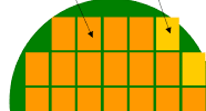
Image Credit: Dev
Optimizing Chip Placement on Circular Wafers Using Breadth-First Search (BFS)
- Semiconductor manufacturing involves fabricating microchips on circular silicon wafers.
- Breadth-First Search (BFS) can be used to optimize chip placement, defect detection, and exposure path planning in wafer lithography.
- The algorithm for BFS chip placement involves starting from the center of the wafer and expanding outward layer by layer to find valid chip positions.
- BFS is also used for defect detection and isolation, as well as optimizing lithography exposure paths in a systematic scanning pattern.
Read Full Article
Like
For uninterrupted reading, download the app